Pages

Showing posts with label VLSI Basics. Show all posts

Deciding between ASICs and FPGAs...


May peace and blessings of the Almighty be upon you all..

Deciding between ASICs and FPGAs requires designers to answer tough questions concerning costs, tool availability and effectiveness, as well as how best to present the information to management to guarantee support throughout the design process.

The first step is to make a block diagram of what you want to integrate. Sometimes it helps to get some help from an experienced field applications engineer. Remember that time is money. Your next move is to come up with some idea of production volume. Next, make a list of design objectives in order of importance. 

These could include cost, die size, time-to-market, tools, and performance and intellectual property requirements. You should also take into account your own design skills, what you have time to do and what you should farm out. Remember that it must make sense financially or you are doomed from the start. 

Time-to-market is often at the top of the list. Some large ASICs can take a year or more to design. A good way to shorten development time is to make prototypes using FPGAs and then switch to an ASIC. But the most common mistake that designers make when they decide to build an ASIC is that they never formally pitch their idea to management. Then, after working on it for a week, the project is shot down for time-to-market or cost reasons. Designers should never overlook the important step of making their case to their managers.

Before starting on an ASIC, ask yourself or your management team if it is wise to spend $250,000 or more on NRE costs (The cost that is invested on the project that cannot recovered back. Example: fabrication charges during ASIC). If the answer is yes and you get the green light, then go. If the answer is no, then you'll need to gather more information before taking the ASIC route. Understand that most bean counters do not see any value in handing someone $250,000 for a one-time charge. They prefer to add cost to the production.

Say your project has a NRE of $300,000, a volume of 5,000, and it replaces circuitry that costs $80. The final ASIC cost is $40. You do some math and determine the break-even point is three years. If you amortize the same design over five years, this could save your company $400,000 even after NRE has been absorbed. 

Another option is to do a "rapid ASIC" using preformed ASIC blocks, which saves time and lowers NRE costs. It could also make sense to convert an FPGA to ASIC directly, which lowers NRE a small amount from the rapid type. 

Now let's say your company will not fund an ASIC effort. That means it's time to consider FPGAs. First, be aware that while the tools are free on the Web for the smaller FPGAs, you'll have to pay for a license file for the ones with high gate counts. The good news is that there are no NRE charges. 

Modern FPGAs are packed with features that were not previously available. Today's FPGAs usually come with phase-locked loops, low-voltage differential signal, clock data recovery, more internal routing, high speed (most tools measure timing in picoseconds), hardware multipliers for DSPs, memory, programmable I/O, IP cores and microprocessor cores. You can integrate all your digital functions into one part and really have a system on a chip. When you look at all these features, it can be tough to argue for an ASIC. 

Moreover, FPGA can be reprogrammed in a snap while an ASIC can take $50,000 and six weeks to make the same changes. FPGA costs start from a couple of dollars to several hundred or more depending on the features listed above. So before you get moving, make sure to enlist some help, get the managers to support you, come up with a meaningful cost estimate, choose the right weapon — be it ASIC or FPGA — and then move into production.

By referring to previous posts in this blog, we will organize the differences between ASICs and Programmable logic devices (CPLDs/FPGAs) in a table which is presented in the next page. The below table discusses about the differences between Programmable devices and ASICs. 

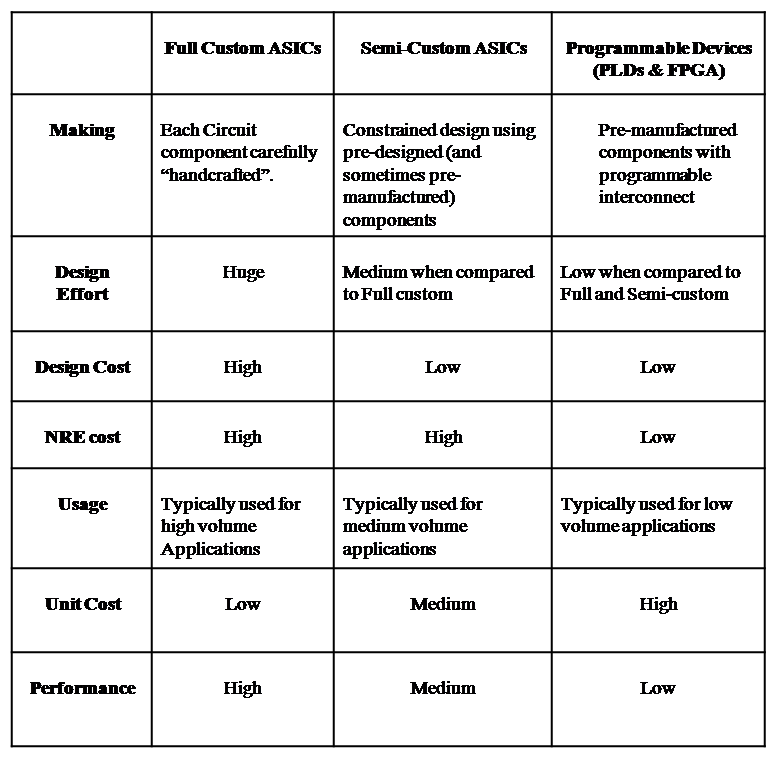
 Please click on the table to enlarge it.

Thank you and lets meet in an another blog post (Insha Allah)

Allah knows best.

Your brother,
Aashiq Ahamed A

Basics of VHDL...


Assalaamu Alaikum,

May peace and blessings of the Almighty be upon you and your family...aamin

VHDL stands for Very high speed integrated circuit Hardware Description Language. It contains two major parts, namely

1. Entity and
2. Architecture
.

Entity is the external view of the project. Here one needs to describe the external features of the project such as Inputs and Outputs.

Architecture is the internal view of the project. Here one needs to describe how those inputs and outputs are  internally connected.

For example, let us consider the below example of Half-Subtractor,


Let us see how to write VHDL code for the above project,

Entity:

entity half_sub is
port (a,b : in bit; diff,bor : out bit);
end half_sub;

One can understand from the above code that entity contains inputs and outputs which are external to the project.

VHDL is a case insensitive language. Entity name can be of any name but care must be taken so that the entity name (here half_sub) should not start with numerics (eg. 24halfsub) and should not be the “keywords” such as xor, and, or, nand, nor, xnor etc.,


Architecture:

Architecture data of halfsub is
Signal s1:bit;
Begin


diff <= a xor b;
s1 <=  not a;
bor <= s1 and b;


end data;

As it is shown above, connection details of the inputs and outputs (which we defined in the entity ) are described in the architecture. Signal is the one which connects two gates and it should be defined between “architecture” and “begin”.

Being a beginner to VHDL one should have a clear vision about the distinction of entity and architecture as it is shown above.

Hope this helps the beginners.

May the Almighty keep us in the straight path always…


Thanks and Regards,
Aashiq Ahamed A

Basics on Programmable devices...


May the peace and blessings of the Almighty be upon you all…


1. When did PLDs come into picture and what is the reason behind that?

         In early 1960s there was discrete logic. Systems were built from lots of individual chips with a spaghetti-like maze of wiring between them. It was difficult to modify such a system after you built it. After a week or two it was difficult to remember what each of the chips was for!

Manufacturing such a system took a lot of time because each design change required that the wiring be redone which usually meant building a new printed circuit board. The chipmakers solved this problem by placing an unconnected array of AND-OR gates in a single chip called a programmable logic device (PLD).

ASICs VS Programmable Devices - The Basics


May the peace and blessings of the Almighty be upon you all…


Is there a difference between ASICs and Programmable devices (like FPGAs/CPLDs)? YES. There are physical differences between them but the purpose of using them is been the same. The purpose is to implement your design and having it in the form of hardware.


To explain this in a very simple way, let us take the following example.

The situation is like this,

WE ARE VERY HUNGRY NOW. WE WANT SOMETHING TO EAT TO FULFILL OUR STOMACH.


Here comes two ways to overcome the above problem,

The first is to prepare some food for ourselves in home and the next way is to approach some restaurants and take the readymade foods available wi them.

Here we have to notice one issue, eventhough they are two different approaches but the purpose of them is the same, i.e. satisfying your hunger.

This is what ASICs and Programmable devices teaches us, the purpose of them is been the same.

ASICs are often referred to us as tailor made ICs.

Just think of this example, you want a shirt now, again there are two ways, they are

1. Go to a tailor shop and give your measurements. The tailor will stitch the shirt for you which will exactly fit to you because the shirt is made from your instructions and

2. Go to a Showroom and pick the shirt for you. Here you are saving time when compared to the previous process (because stitching time will be more) but sometimes shirt/pant will not exactly fit into body because you may be short or tall. Then you have to do some alternations.

ASICs and Programmable devices are exactly the same like the above example. Implementing your designs in an ASIC will take more time when compared to Programmable devices because you have to design your circuits, approach a vendor (just like you approach a tailor to stitch your shirt/pant), make a chip which will replicate your design. On the other hand using Programmable devices we can save time because, to design your circuits, buy an already manufactured Programmable device, and implement your design.
  
If you see here, the biggest advantage ASICs have over their counterparts is that you will get exactly your design fed into an IC without any extra circuits inside it. Just like a tailor made shirt or preparing your food. You know your taste and you will prepare food according to you/your family members. Isn’t it?

On the other side, implementing your design in a Programmable device will not only have your design but also some extra circuits inside it. It will suit only for some standard customers just like ready made shirts will suit into people of standard sizes and not to all of them or eating in restaurants where you will feel the food not upto your taste..

If you ask me what I will use for my design, without any question I will go for the seamless ASIC technology.

BECAUSE HOME MADE FOOD IS BETTER THAN HOTEL FOOD. ISN’T IT?


Thanks and Take care,

May the Almighty guide us in the straight path always…Aamin.

God knows best…


Your brother,
Aashiq Ahamed A
aashiq.ahamed.14@gmail.com


The Basics - VLSI Classification...


May the peace and blessings of the Almighty be upon you all…


Having seen about classification of ICs in the last post, let’s move ahead and categorize fig 1.1 into two major parts,

  • Core VLSI
  • Application VLSI.


The reader should be aware that this is not the way people generally practice or explain. I am doing this here for the sake of easy understanding.


Core VLSI:
This is the one which talks about making (design and fabrication) an IC from the core, i.e. starting from preparing the substrate etc...

Application VLSI:
This is the one which talks about programming or configuring a programmable chip.


Learning VLSI will be easy if we approach it in the below mentioned ways,

  1. First, Learning How an IC is been designed and fabricated.
  2. Second, How to configure a Programmable device (particularly CPLD and FPGA)

VLSI concepts will be easily understood if one tries to find out answers for the above questions. 

Hence, just set the above two points as your targets in learning VLSI concepts and try to find out the answers for above questions.

And yes, that is what we are trying to achieve in future posts (Insha Allah), i.e. trying to find out answers for above questions, how to design a IC and how to configure a programmable device.  

Insha Allah (God Willing), in the next post we will go ahead and learn the differences between ASICs and Standard Products (more specifically Programmable devices).

Thanks and Take care,

May the Almighty guide us in the straight path always…Aamin.

God knows best…


Your brother,
Aashiq Ahamed A
aashiq.ahamed.14@gmail.com

The Basics --- IC Classification...


May peace and blessings of the Almighty be upon you all…


Having seen in the last article that VLSI is the technique that deals with ICs, let’s go ahead with IC classification. 

Whatever may be the ICs that we see in the modern world, they are classified into two major categories, ASICs and Standard Products, as shown in the figure below, 


1. ASIC means Application Specific Integrated Chip. 

Name tells the story. These kinds of ICs are used only for specific applications. For example, let us take the ICs used in a particular model of a mobile phone. You can’t use that ICs in any other model or in any other manufacturer’s phone. These ICs are made only for that particular model of the mobile phone.

In other words, these ICs are application specific; you can’t use them for other applications.  


2. On the other hand, STANDARD PRODUCTS are the one which can be used for different applications. 

For example, take the 74 series ICs. The 7486 ex-or gate IC which is used to construct a Half Adder is also used is construct different circuits like fulladder, parity generator etc., It is not limited to one particular application. 

Similarly, take the FPGA, if you write the program for half adder and dump it in the FPGA, it will work as a half adder. The same FPGA will work as a full adder, parity generator etc.. if you write corresponding programs. Thus FPGAs are not limited to one particular application and they are used for different applications. 


3. The major difference between the Standard ICs and Programmable devices is that, standard ICs are used for different applications but they can not be re-programmed (can we re-program a 7486?) whereas programmable devices are used for different applications and they can be re-programmed also.   


For our easy understanding in learning VLSI, we will categorize the above figure into two parts, which we will see in the next article. Insha Allah.   

May the Almighty guide us in the right path always…aamin. 

Allah(swt) Knows best…


Your brother,
Aashiq Ahamed A

Introduction....


May Peace and blessings of the Almighty be upon you...

Please Note:

Before starting this post, one important thing I would like to address. In this post and future, you may come across a lot of new technical terms. All I can say is, just skip them if you can't understand and continue reading. Over the period of time when we see detailed explanation of them you will be able to understand and relate to previous posts. Insha Allah…   

Lets go ahead now...

1. What does VLSI mean?

VLSI stands for Very Large Scale Integration. As the name suggests, when a large number of transistors (say for example greater than 10,000 transistors) packed in an Integrated chip then it is said to be following VLSI technology. To be more precise, making an IC with large number of transistors is called VLSI. Today’s sophisticated Integrated Chips have millions of transistors inside them.

But I used to say, VLSI means making a Simple IC (also), because if we can’t understand how a simple IC is been made and then how come we learn about multi-million transistor design? So let us start with a simple IC, how it is been designed and made, and then focus on packing multi-million transistors.    

But VLSI has another side to it also, configuring programmable devices such as PLDs (PLAs, PALs, PROMs and CPLDs) and FPGAs are also considered to be a part of VLSI.


2. Why is it so?

As far as I am concerned there are two major reasons behind it.

a) Motive of both of them is the same (or in other words, the results they try to achieve is the same).

For example, let us assume that we need a EX-OR circuit; there are two ways of getting it. The first, get the EX-OR circuit by designing (using CMOS processes, layout etc., which we will see later) and fabricating. The resultant IC from fabrication contains EX-OR circuit.

The second, take a programmable device, describe the behavior of EX-OR circuit (by writing codes in VHDL/Verilog HDL or through schematic) and dump it in the programmable device. Now your programmable device will work as EX-OR circuit.     

Since both of them produce same result, Programmable devices are said to be part of VLSI.

b) The approach towards the Motive is almost same.

For example, when I say, write the code and dump (Configure) it in the programmable chip, that does not mean there are only two steps. In-between writing the code and dumping, there are other steps need to be followed like synthesis, placement and routing etc (which we will see later). These steps are called Design Steps. 

Similarly to make an IC on our own, we need to follow certain steps (Design Steps). These steps are almost similar to the steps that we follow in configuring programmable devices.

Since both of them follow similar steps to achieve their motive, programmable devices are said to be a part of VLSI technique.

There may be some other reasons also like prototyping etc., which we will see later, Insha allah…


3. Where does VLSI techniques used?

Just look around you. Look at the computer you are using, look at the IPOD you are using, look at the mobile phones you are using, etc etc. They all contain ICs packed with millions of Transistors. You can't imagine electronic products without VLSI techniques.  


4. Why VLSI is so important?

By this time you would have understood that. If todays's world heavily dependent on state of the art Electronic goods, then those goods heavily depend on sophisticated Multi-Million transistor ICs. Thus the importance. You can't just skip VLSI techniques and claim to be a better Electronics Engineer.


5. Is VLSI a kind of course which one needs to learn separately?

It depends on the educational institution one studied/studying. If you are from the stream of Electronics, Electrical and Instrumentation, then you already got a glimpse of it in your college days. Or if you are a student then you are learning it now. 

Most of us learned about or learning about terms like CMOS, ASICs, Lambda based rules, digital electronics, HDLs, Layout etc., which will obviously lead to VLSI. 

Having said that, VLSI tools could not be found in most of the educational institutions, primarily due to cost involved with them. In that case an outside course will help a lot. 


Let me finish by saying this, VLSI is not at all a complex thing to learn. It is so cool and fun. That is what I will try to do in future posts, ie. presenting VLSI in the easiest way possible. Insha Allah...

Do send in your comments if you face any difficulty in understanding...

God knows best...

Thanks,


Your brother,
Aashiq Ahamed A